Revitalizing the need for analog chip design, researchers from the Indian Institute of Science (IISC) describe a framework for future analog AI chips.
As the industry continues to push for lower power and higher performance processing for machine learning (ML) and artificial intelligence (AI), a plethora of new concepts and technologies have taken center stage. Amongst these, analog computing has been revived as an exciting approach to more efficient processing.
Still, the technology is relatively new for this given application, and there is significant room for improvement. This week, researchers from the IISC published a new paper describing a novel framework for the future of scalable analog AI chips.
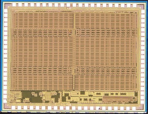
IISC’s ARYABHAT-1 chip. Image used courtesy of NeuRonICS Lab, DESE, IISc
This article will discuss the benefits of analog computation for AI, some challenges facing the technology, and the new research from IISC.
Why is there a Shift to Analog?
Analog computation is a technology that predates digital computing but had largely been forgotten as digital took off. Now, researchers are again looking to analog, and this time it appears to have digital beaten in several ways.
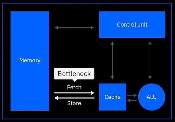
A conventional von Neumann architecture is bottlenecked by data movement. Image used courtesy of IBM
As data rates have gotten faster, process nodes smaller, and global interconnects longer, an emerging trend in the industry has been the significant impact of data movement energy.
Increasing parasitics have caused the physical movement of data in and out of memory has become one of the most significant contributors to overall chip power consumption. Couple this with ML, an extremely data-intensive application, and we find that the von Neumann architecture is no longer well suited for AI/ML.
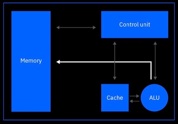
Analog AI brings the processing directly to the memory. Image used courtesy of IBM
Instead, analog computation allows for in-memory computation, where data can be processed where it is stored. The major benefit is the significant decrease in data movement overall, which reduces overall energy expenditure.
This way, analog AI can offer power efficiency improvements up to 100x compared to traditional digital electronics for AI/ML applications.
Challenges for Analog AI Scaling
Despite its efficiency benefits, analog computing still faces several challenges before it can be a legitimate competitor to digital computing.
One of the key challenges in the design of analog computing for AI/ML is that, unlike digital chips, testing and co-design of analog processors is difficult. Traditionally, VLSI (very-large-scale integration) design can consist of millions of transistors, but engineers can synthesize the design by compiling high-level code. This capability allows the same design to be easily ported across different process nodes and technology generations.
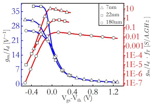
Transconductance (gm/Id) as a function of (Vgs–Vth) at different process nodes. This plot shows the challenges in easily scaling analog designs. Image used courtesy of Kumar et al
Analog chips, however, don’t scale as easily due to differences in transistor biasing regimes, temperature variations, and limited dynamic range. The result is that each new generation and process node needs to be individually customized and re-designed. This result not only makes the design more time-consuming and expensive, but it also makes it less scalable, as transitions to new technology generations require a lot more manual work.
For analog AI to make it mainstream, the challenges towards design and scalability need first to be solved.
IISC’s Framework to Scale AI
To solve this problem, researchers at the IISC have proposed a new framework for scalable analog compute design in their most recently published paper.
The key concept of their work revolves around the generalization of margin propagation (MP), which is a mathematical tool that has previously shown value in synthesizing analog piecewise-linear computing circuits using the MP principle.
Out of this generalization, the researchers developed a novel shape-based analog computing (S-AC) framework that allows the researchers to approximate different functions commonly used in ML architectures.
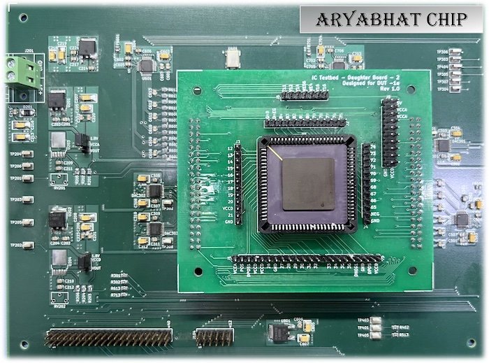
Test setup for the chip built off of the proposed analog framework. Image used courtesy of NeuRonICS Lab, DESE, IISc
The result was a framework that successfully could trade off accuracy with speed and power, like digital designs, and also be scaled across different process nodes and biasing regimes.
As a proof-of-concept, the researchers implemented a number of S-AC circuits to represent common mathematical functions in ML in several different processes. In doing this, the researchers successfully used circuit simulations to demonstrate that the circuit I/O characteristics remained reasonably the same across both a plan 180 nm CMOS process and a 7 nm FinFET process.
With the new framework, the researchers hope to have created something that will allow for more scalable and cost efficiency analog AI designs in the near future.

