STMicroelectronics and MACOM announced the successful production of RF GaN-on-Silicon technology, hoping to solve GaN production challenges for RF components.
As 5G and 6G technologies are being developed, they are proving to represent a significant challenge for the underlying circuitry and hardware. To keep up with the rapid advancements in wireless technology, engineers are evaluating many new technologies on the hardware level.
One of these technologies is gallium-nitride on silicon (GaN-on-Si). This technology is of interest because it has the potential to marry the high-performance capacity of GaN with the manufacturability and cost of Si.

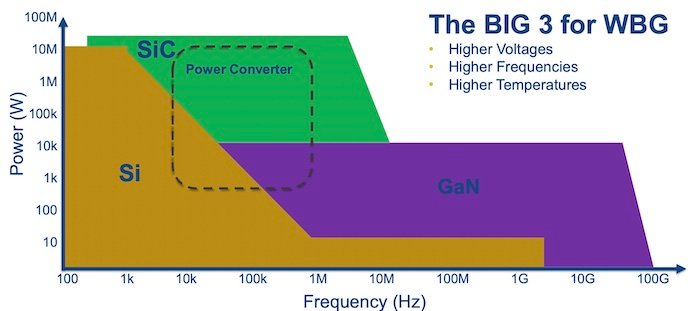
A comparison of power and frequency of wide-bandgap (WBG) semiconductor materials. Image used courtesy of Kemet
Recently, STMicroelectronics announced that, in collaboration with MACOM Technology Solutions, it has successfully produced RF GaN-on-Si prototypes.
This article will look at GaN-on-Si technology, its potential in RF applications, and the news from ST and MACOM.
GaN and Possible RF Challenges
It has been well documented that WBG semiconductors such as GaN are among the most promising technologies for achieving high power efficiency in future RF and power electronics.
GaN is uniquely poised for power electronics due to its material properties such as:
- Large bandgap
- High electron saturation velocity
- Large breakdown field
- High mobility
Together, these properties could offer significant performance advantages of high efficiency, thermal tolerance, and reliability instead of conventional Si solutions.

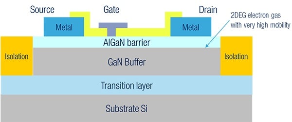
Structure of a GaN HEMT. Image used courtesy of STMicroelectronics
For example, in RF applications, GaN offerings highly outperform conventional laterally-diffused metal-oxide-semiconductor (LDMOS) technologies that are the traditional choice for components such as power amplifiers (PA). With GaN, RF PAs could achieve higher output power and efficiencies, making for smaller and more performant 5G and 6G hardware.
However, a notable challenge with GaN is that it does not benefit from the same economies of scale that Si does. Since Si is so well studied and has been commercialized for decades, the manufacturing processes that are in place for Si products allow for high volume and low-cost offerings, even at complex technology nodes.
GaN, on the other hand, is a relatively new technology without the manufacturing infrastructure necessary to meet the same costs that Si offers.
GaN-on-Silicon—A GaN Manufacturing Solution
To solve that problem, many have turned to GaN-on-Si technology.
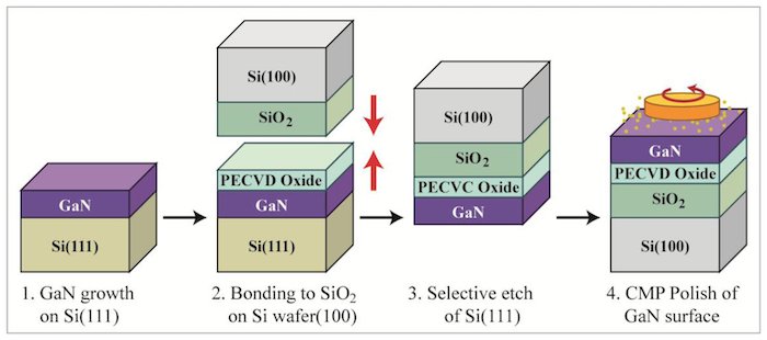
GaN-on-Si is a manufacturing process in which GaN devices can be grown directly on top of conventional silicon substrates. In this process, a GaN epilayer is grown on top of the Si substrate, allowing for the existing silicon manufacturing infrastructure to mass-produce GaN devices at low costs.

Example GaN-on-Si manufacturing process for photonics. Image used courtesy of Xiong et al
However, this process hasn’t been without challenges. It has proven exceptionally difficult to grow high-quality GaN out of Si substrates due to mismatches in the two materials’ lattice structures. Due to this, GaN-on-Si is not widely available, at the moment, for RF, but the industry continues to invest heavily in the technology.
ST and MACOM Team-up for RF GaN-on-Si
This week, ST and MACOM made headlines in the industry when they announced their successful production of RF GaN-on-Silicon prototypes.
While not many explicit details are available about this news, the companies are purporting that the prototype wafers and devices they’ve developed have achieved comparable cost and performance to conventional LDMOS solutions. With the successful production of these prototypes, they plan to move the products into the qualification and industrialization stages within 2022.
This news can be significant as it represents major players in the field delivering a concerted effort into GaN-on-Si technology and having success. Through this, the industry is closer to obtaining the performance benefits of GaN while achieving the economies of scale of Si.
In the end, this achievement can result in engineers hopefully being able to leverage the better performance for less, making for better circuits, systems, and products.

