High expectations are placed on today’s microcontrollers (MCUs). To keep pace, MCU companies are beefing up peripherals mixes and security, while some are even adding time-sensitive networking (TSN).
There’s no doubt that today’s advanced MCUs are at the heart of every kind of embedded system across hundreds of application segments. Even though the major MCU already offers a seemingly endless number of combinations of compute power, peripheral mix, and memory options, they continue to evolve and improve their offerings across all fronts.
In this article, we’ll round up a selection of new Arm core-based MCUs that bring new systems capabilities into play for applications including TSN for industrial systems, IoT, home automation, and consumer white goods.
NXP Crossover MCU Embeds TSN Switch
Industry 4.0 is characterized by high network traffic and the exchange of big data over a multi-protocol network. The problem is getting industrial networks to seamlessly work together can be difficult—especially when time-sensitive communication is required.

TSN provides critical Ethernet determinism for Industry 4.0 applications. Image used courtesy of NXP Semiconductors
Although Ethernet has been widely adopted for industrial systems, it does not provide deterministic communication on its own. Fortunately, a set of IEEE 802 standards collectively called TSN-enabled Ethernet is deterministic by default.
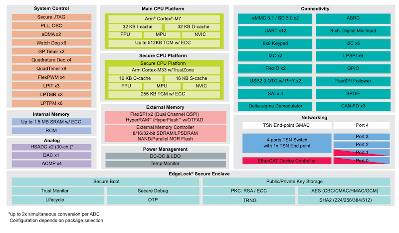
With all that in mind, in May NXP Semiconductors unveiled what it claims is the first-ever MCU that integrates a Gbps TSN switch. Called the i.MX RT1180 crossover MCU, the dual-core device embeds an 800 MHz Arm Cortex-M7 core and a 240 MHz Cortex-M33 core. According to the company, the i.MX RT1180 provides the needed multi-protocol connectivity to achieve time-sensitive and real-time communications simultaneously. This should enable engineers to easily create unified and secure industrial IoT communication environments.
The chip’s ability to support multiple protocols is perhaps its most important feature. It supports the latest generation of TSN standards-compliant to IEC 60802 for industrial automation. Among TSN-based protocols supported are OPC UA Pub-Sub, Profinet over TSN and CC-Link IE TSN.

Block diagram of the i.MX RT1180 crossover MCU. Image used courtesy of NXP Semiconductors (Click image o enlarge)
Up to five Gbps ports are provided, including 4x ports on the TSN switch (Layer 2) and 1x port on the TSN endpoint controller. Meanwhile, real-time industrial Ethernet protocols are likewise supported, such as Profinet, EtherCAT, CC-Link IE Field, Ethernet/IP, HSR, and more.
For security, the i.MX RT1180 includes an NXP EdgeLock secure enclave, a preconfigured, self-managed and autonomous on-die security subsystem that eliminates the difficulty that is associated with implementing robust, system-wide security intelligence for industrial IoT applications.
According to NXP, the MCU offers an integrated solution to a wide range of industrial operations including I/O management, motor control, compact motion control, or gateway applications. The i.MX RT1180 is also suitable for automotive connectivity applications where the i.MX RT1180 could act as an intelligent switch between different automotive ECUs.
Renesas MCUs Certified by NIST Crypto Program
Security is a vital feature for MCU-based designs, and for IoT systems in particular because they are, by definition, connected systems. One way MCU vendors are keeping pace is by certifying their products in line with the security standards maintained by various standardization bodies in the industry.
Along those lines, in May Renesas Electronics announced that its RA family of 32-bit Arm Cortex-M MCUs was certified by the National Institute of Standards and Technology (NIST) Cryptographic Algorithm Verification Program (CAVP). Specifically, the security engines within the company’s RA6M4, RA6M5, RA4M2, and RA4M3 MCUs were certified under CAVP. This adds to several other IoT security features in the RA MCU chips. The company says that the drivers needed to use the certified SCE9 Protected Mode are added to the RA Family Flexible Software Package (FSP) v3.6.0 and later.
Renesas says the RA MCUs received the PSA certified level 2 and security evaluation standard for IoT platforms (SESIP) certifications in the past. But this new NIST CAVP certification is geared toward certifying the cryptographic algorithms including multiple modes of Advanced Encryption Standard (AES), hashing, Rivest Shamir Adleman (RSA), and Elliptic Curve Cryptography (ECC) key generation and authentication that are embedded in the security engines of the RA MCUs.
With this new certification, the MCUs are provided with a security key management tool that is responsible for preparing keys for secure installation, updates, supporting development, production provisioning, and key updates for products in the field.
Renesas says that an independent evaluation was done recently comparing the RA MCU’s SCE9 Protected Mode operation to a selection of industry-leading secure elements in the industry. A white paper detailing the evaluation is available.
Renesas Shows Off Upcoming Arm Cortex-M85-based MCU
While equipping its current crop of MCUs with the latest security mechanisms, Renesas is looking ahead to its next set of offerings by providing a demo of its upcoming ArmCortex-M85 processor core-based MCU. At Embedded World 2022 last month, Renesas provided its first live demonstration of the MCU.

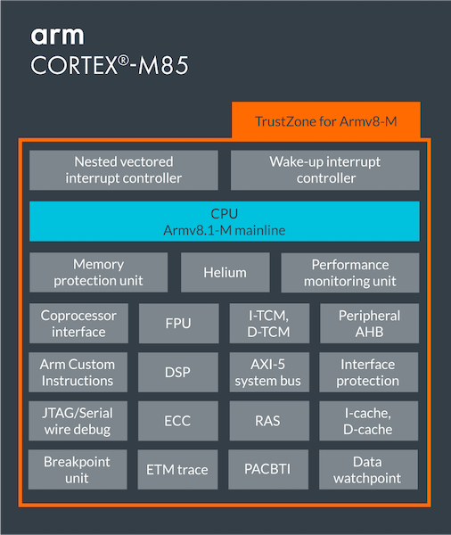
Block diagram of the Arm Cortex-M85 processor core. Image used courtesy of Arm
Announced by Arm in April, the Arm Cortex-M85 processor core features Helium technology. With advanced DSP/ML capabilities the processor accelerates compute-intensive applications, says Renesas. According to the company, its upcoming M85-based RA family of MCUs will provide fully deterministic, low latency, real-time operation for demanding application needs across numerous markets. Renesas says new MCUs are planned for release in 2023.
New Toshiba MCUs for Consumer Appliances and More
Last but not least, mid-Spring saw Toshiba announcing 21 new MCUs in its M3H group as new products in the company’s TXZ+ Family Advanced Class of devices. Built on a 40 nm process, the M3H group MCUs embed a 120 MHz Arm Cortex-M3 core. For memory, the chips provide up to 512 KB of code flash and up to 32 KB of data flash memory with 100k write cycle endurance.
The new MCUs also provide a rich set of interface and motor control options. Among these are UART, I2C, Encoder, and Programmable Motor Control. Toshiba says the M3H group devices are suited for a wide range of applications including home appliances, motors, and industrial equipment. A digital LCD driver is integrated and it is expected to shrink the number of components engineers will need to enable a display function and facilitate contrast adjustment.

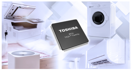
The new M3H MCUs are well suited for applications in home appliances and consumer electronics. Image used courtesy of Toshiba
Meanwhile, the new MCUs also feature a high-speed, high-precision 12-bit analog-to-digital converter (ADC). The ADC allows individual samples and holds times to be set for each of the ADC’s 21 ADC input channels.
Toshiba says the ADCs also can be used for controlling AC motors and brushless DC motors. This is done in combination with an advanced programmable motor control circuit on the MCUs that can operate synchronously with the 12-bit ADC.
Self-diagnosis functions are embedded in the devices for ROM, RAM, ADC, and Clock units on the chips. This helps engineers achieve IEC60730 Class B functional safety certification.
The Ultimate System-on-Chip?
Since they provide so many systems functionally, in many ways, MCUs are the ultimate system-on-chip. However, MCU vendors seem to keep finding new ways to enhance the processing power, peripheral mix, and security features of their MCU product families.

